1555F Series enclosures have several innovative features that provide excellent functionality
Understanding BJT Transistors and How to Practically Use Them in Your Designs

Transistors are one of the very important components used in electronic circuit constructions. These humble components can almost be found everywhere; from simple relay driver circuits to complex motherboard circuits, transistors prove their presence. In fact, your microcontrollers and microprocessors are nothing but a collection of a large number of transistors synthesized to perform a collective operation. Do remember that many switching devices like BJT, MOSFET, IGBT, SCR, TRIAC, DIAC, etc. can be collectively called transistors. But, the most basic (oldest) of the transistor is the BJT Transistor, hence in this article, we get into details of that, you can use the links to learn more about other power switches.
BJT is the short form of Bipolar Junction Transistor, it is a solid-state current-controlled device which can be used to electronically switch a circuit, you can think of it as your normal Fan or Light switch, but instead of you turning it on manually it can be controlled electronically. Technically speaking, BJT is a three-terminal device with an Emitter, collector, and a base pin, the current flow through the emitter and collector are controlled by the amount of current applied to the base. Again you can think of emitter and collector as the two ends of your switch and instead of pressing the switch, we have the base pin which can receive the control signal. But how exactly does it work? And how to use a transistor to build interesting circuits? That's exactly what we are going to answer in this Tutorial.
Symbol of BJT Transistors
Let's start with the symbol of transistors so that you can identify them in a circuit. The below diagram shows the symbols of the two types of transistors. The one on the left is the symbol of the PNP transistor and the one on the right is the symbol of the NPN transistor. As I said, you will be able to see the three terminals Emitter, Collector, and Base for both the type of Transistor.
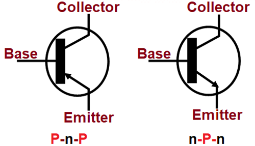
The difference between the PNP and NPN transistors is that the arrow mark at the emitter end if you have noticed, the arrow in the PNP transistor is mentioned as moving from the emitter to the base whereas in the NPN transistor the arrow will be moving from the base to the emitter. The Direction of the arrow represents the direction of current flow in the transistor, in PNP the current will be flowing from emitter to base, similarly in the NPN transistor current will be flowing from the base to emitter.
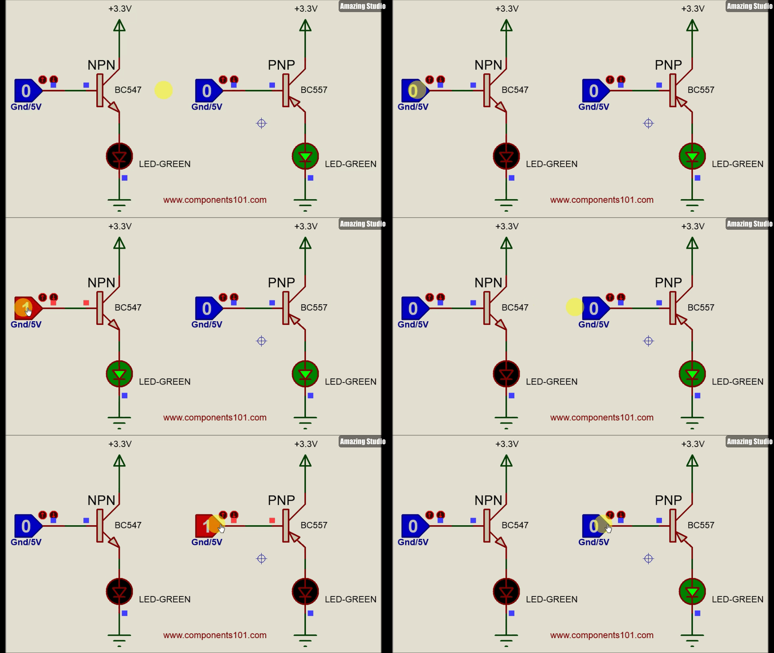
Another important difference is that an NPN transistor remains open until it receives a signal on the base pin while a PNP transistor remains closed until a control signal is provided to the base pin as shown in the above GIF file.
Construction of Bipolar Junction Transistor
The BJT is formed by three layers of semiconductor materials, if it is a PNP transistor, it will have two P-type regions and one N-type region, likewise, if it is an NPN transistor, it will have two N-type regions and one P-type region. The two outer layers are where the collector and emitter terminals are fixed and the base terminal is fixed at the center layer.
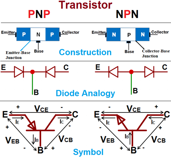
The construction can simply be explained with a two diode analogy for transistor as shown in the above image, if you want to learn more about diodes, you can consider reading his article. Consider the two diodes connected with each other using the cathode, then the meeting point can be extended to form the base terminal and the two anodes end acts as the collector and emitter of a PNP transistor. Similarly, if you connect the anode ends of the Diode then the meeting point of the anodes can be extended to for the base terminal and the two cathode ends act as the collector and emitter of the NPN transistor.
Working of Transistor (BJT)
Practically the working of a transistor is very simple, it can be used as a switch or as an amplifier. But for basic understanding lets start with how transistor as a switch works in a circuit.
When a control voltage is provided to the base pin, the required base current (IB) flows into the base pin which is controlled by a base resistor. This current turns on the transistor (switch is closed) and allows the current to flow from collector to emitter. This current is called the collector current (IC) and the voltage across the collector and emitter is called VBE. As you can see in the image, we are using a low-level voltage like 5V to drive a higher voltage load of 12V using this transistor.
Now for the theory, consider an NPN transistor, the BE junction is forward biased and the CB junction is reverse biased. The width of the depletion region at the Junction CB is higher when compared with the depletion region of the Junction BE. When the BE junction is forward biased it decreases the barrier potential, hence the electrons start flowing from the emitter to the base. The base region is very thin and it is lightly doped when compared with other regions, hence it consists of a very small number of holes, the electrons that are flowing from the emitter will recombine with the holes present in the base region and start to flow out of the base region in the form of the base current. A large number of electrons that are left will move across the reverse bias collector junction in the form of the collector current.
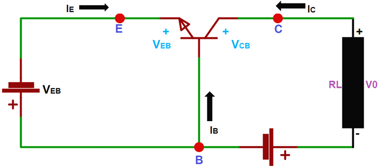
Based on the Kirchoff’s Current Law, we can frame the current equation as
IE = IB + IC
Where, IE, IB, and IC are the emitter, base, and collector current respectively. Here the base current will be very small when compared with emitter and collector current, therefore, IE ~ IC
Similarly, when you consider the PNP Transistor, they operate in the same way as the NPN transistor, but in NPN transistors the majority charge carriers are holes (Positively charged particle) but in the NPN transistor the charge carriers are the electrons (negatively charged particle).
Characteristics of BJT
BJT can be connected in three different configurations by keeping one terminal common and using the other two terminals for the input and output. These three types of configurations respond differently to the input signal applied to the circuit because of the static characteristics of the BJT. The three different configurations of BJT are listed below.
- Common Base (CB) configuration
- Common Emitter (CE) configuration
- Common Collector (CC) Configuration
Among these, the Common Base configurations will have voltage gain, but no current gain, whereas the Common Collector Configuration has current gain, but no voltage gain and the Common Emitter Configuration will have both current and voltage gain.
Common Base (CB) Configuration
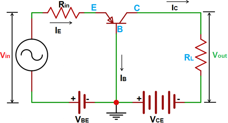
The Common Base configuration is also called as the grounded base configuration, where the base of the BJT is connected as a common between both the input and output signal. The input to the BJT is applied across the Base and Emitter Terminals and the output from the BJT is obtained across the Base and Collector terminal. The input current (IE) flowing through the emitter will be quite higher when compared with both the Base current (IB) and the Collector Current (IC) as the emitter current is the sum of both the Base current and Collector current. Since the collector current output is less than the Emitter current input the current gain of this configuration will be unity (1) or less.
Input characteristics
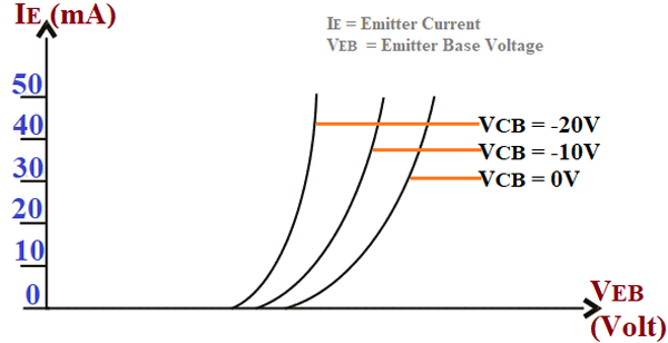
The input Characteristic curve for the Common Base configurations is drawn between the emitter current IE and the voltage between the base and emitter VEB. During the Common base configuration, the Transistor gets forward biased hence it will show characteristics similar to that of the forward characteristics of a p-n diode where the IE increases for fixed VEB when VCB increases.
Output Characteristics
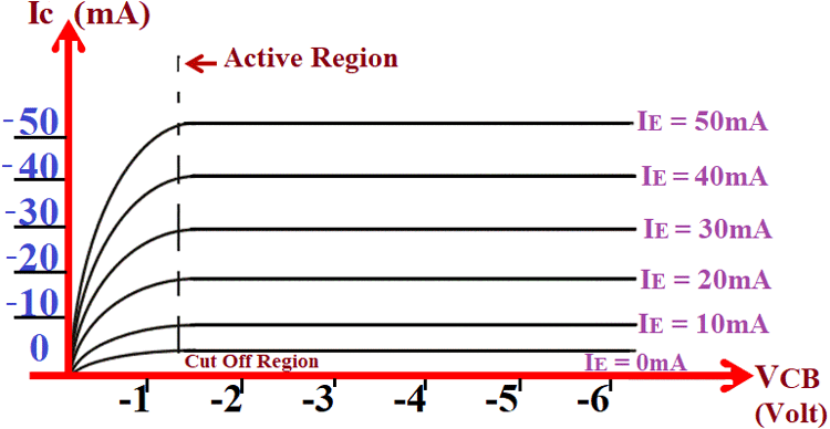
The output characteristics of the Common Base configuration are given between the collector current IC and the voltage between the collector and base VCB, here the emitter Current IE is the measuring parameter. Based on the operation, there are three different regions in the curve, at first, the active region, here the BJT will be operating normally and the emitter junction is reverse biased. Next comes the saturation region where both the emitter and collector junctions are forward biased. Finally, the cutoff region where both emitter and the collector junctions are reverse biased.
Common Emitter (CE) Configuration
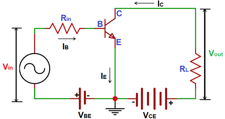
The Common Emitter Configuration is also called the grounded emitter configuration where the emitter acts as the common terminal between the input applied between the base and emitter and the output obtained between the collector and the emitter. This configuration produces the highest current and power gain when compared with the other two types of configurations, this is because of the fact that the input impedance is low as it is connected to a forward-biased PN junction whereas the output impedance is high as it is obtained for the reverse-biased PN junction.
Input Characteristics
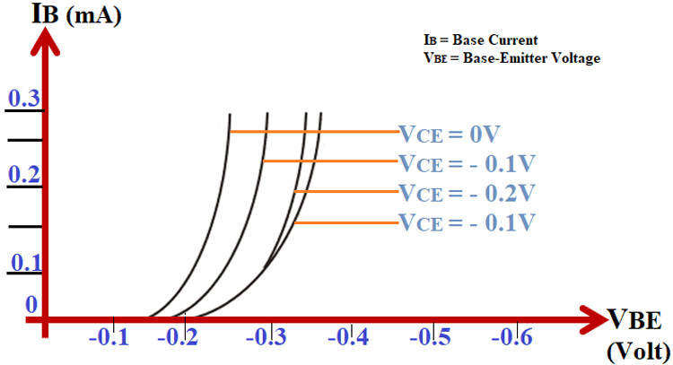
The input characteristics of the Common Emitter configuration are drawn between the base current IB and the voltage between the base and emitter VBE. Here the Voltage between the Collector and the emitter is the most common parameter. If you could see there will not be much difference between the characteristic curve of the previous configuration except for the change in parameters.
Output Characteristics
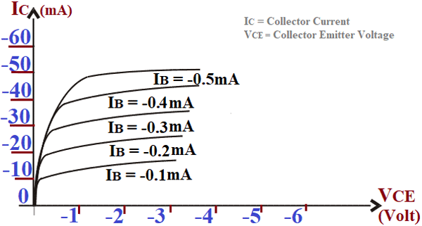
The output characteristics are drawn between the Collector Current IC and the voltage between the collector and the Emitter VCE. The CE configuration also has the three different regions, in the active region the collector junction is reverse biased and the emitter junction is forward biased, in the cut-off region, the emitter junction is slightly reverse biased and the collector current is not completely cut off, and finally, in the saturation region, both the collector and the emitter junctions are forward biased.
Common Collector (CC) Configuration
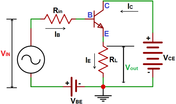
The Common Collector Configuration is also called the grounded Collector configuration where the collector terminal is kept as the common terminal between the input signal applied across the base and the emitter, and the output signal obtained across the collector and the emitter. This configuration is commonly called as the Voltage follower or the emitter follower circuit. This configuration will be useful for impedance matching applications as it has very high input impedance, in the region of hundreds of thousands of ohms while having relatively low output impedance.
Application of Bipolar Junction Transistors (BJT)
BJT can be used in various kinds of applications such as logic circuits, amplification circuits, oscillation circuits, multi-vibrator circuits, clipping circuits, circuits of the timer, time delay circuits, switching circuits, etc.
Types of packages
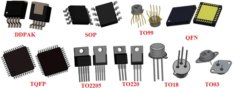
For the better usage in different kinds of applications, BJTs are available in various packages such as TO-3, TO-5, TO-8, TO-18, TO-36, TO-39, TO-46, TO-52, TO-66, TO-72, TO-92, TO-126, TO-202, TO-218, TO-220, TO-226, TO-254, TO-257, TO-258, TO-259, TO-264, and TO-267. You can also check our different types of IC package articles to know the popular types and their names.


